

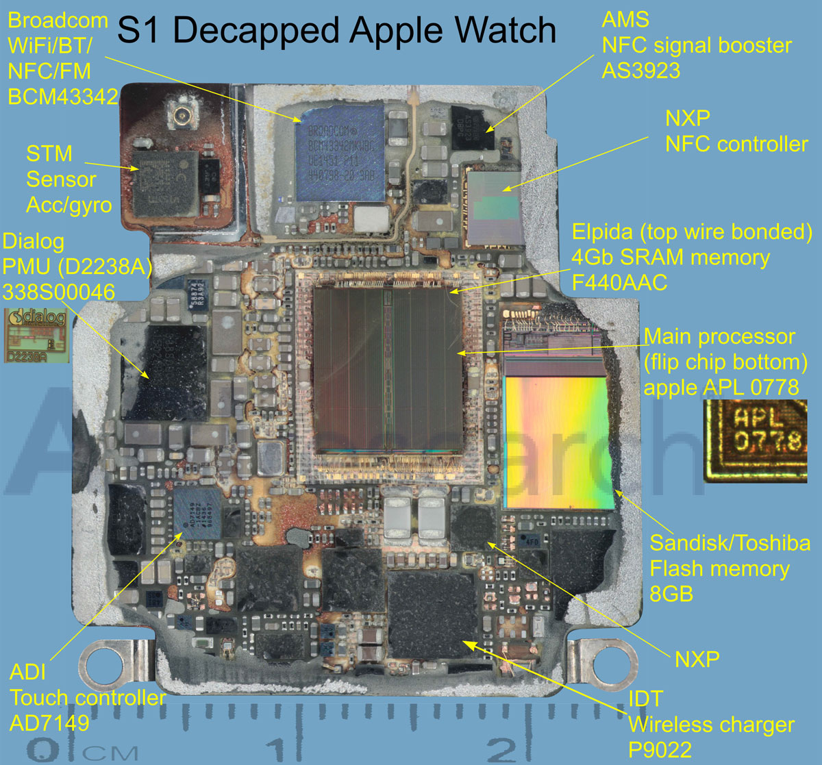
Deconstructing the new Apple watch is not a game for amateurs. ABI Research’s TeardownIQ reveals a design centered on a custom Apple Processor (APL 0778) but includes Broadcom (BCM43342), Dialog PMU, NXP (NFC controller), and AMS (NFC booster) connectivity, IDT wireless charger receiver, Elpida RAM, SanDisk / Toshiba Flash memory, STM sensors, and a couple ADI capacitive touch solutions.
First Look at Apple Watch PCB (Graphic: Business Wire)
“Judging by the complexity of the printed circuit board (PCB), and the number of parts on the PCB, one might think the Apple watch is a full-fledged cellular connected watch but in fact connectivity is limited to Wi-Fi, Bluetooth, and NFC.”
“The design is an obvious variation from Apple’s smartphones, with many high-end functions / chips included that normally would not be found in a simple watch,” comments Jim Mielke, VP Engineering at ABI Research and head of the TeardownIQ group. “Judging by the complexity of the printed circuit board (PCB), and the number of parts on the PCB, one might think the Apple watch is a full-fledged cellular connected watch but in fact connectivity is limited to Wi-Fi, Bluetooth, and NFC.”
A few of key surprises in the design are two touch controller design wins for ADI, and the IDT wireless charging receiver. ADI has not seen a lot of design wins in mobile devices over the last 3 to 5 years but it seems to have a new focus as it has shown up in this Apple design and its sensors were revealed in a few other very recent teardowns.
These findings are part of ABI Research’s Teardowns Market Research (https://teardowns.abiresearch.com/), which includes Parts Lists, High-Res Photos, and Power and Performance Testing.


